How to design PCBs correctly, to reach boards which are cost-effective to produce and to populate? Which are the most important PCB design principles? What about production technology of PCB? We have prepared for you a series of articles about the PCB´s design.
This is an archive article published 04/10/2017. Some information may no longer be up to date and in line with the current state. Please contact us in case of interest.
PCBs are integral part of all electronic devices. Their basic function is to create a conductive connection between the pins of the individual components. PCBs first appeared in late '60s, when there were the first rules for their design and production drawn up - IPC standards. The standard IPC-2221 "Generic Standards on Printed Design".
What is the first step when designing PCB?
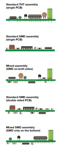
In electronic praxis, 3 types of components are used and possibilities of their soldering are:
- components with leads "Through Hole" – TH (axial, radial), can be soldered by hand or by wave,
- leaded components for a surface mount – "Surface Mount Devices" – SMD, which can be soldered in a reflow oven or by a wave,
- no-lead components for a surface mount – "Surface Mount Devices" – SMD, which can be soldered in reflow oven.
With these three types of components you can create an electronic device in which these components are placed on a carrier - printed circuit boards (PCB). Components can be populated on a PCB either on one side (SMD, TH or a combination of both) or on both sides (TH only on a top side, SMT on both). When the PCB is designed, there must be placement of components on PCB and type of soldering technology considered, because different rules apply when soldering by solder wave and different for soldering in the reflow oven.
1. Soldering by solder wave
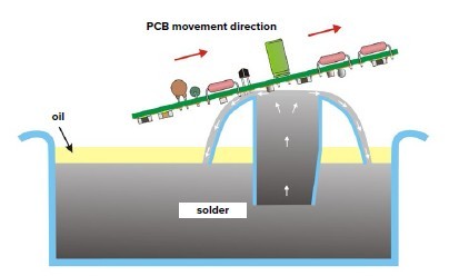
If we want to solder components on bottom of PCB by solder wave, we must ensure that during the soldering process components will not fall off. SMT components on the upper side will be populated into a solder paste, then soldered in a reflow open. SMT components on the bottom of the PCB will be bonded by a glue and then TH components will get into holes in a PCB. SMT components in a glue and TH components will be soldered by a solder wave.To populate components with leads on one side of the PCB is easy process as only leads are sink into the solder wave and conductive joint is created. Interesting is it in case of SMD components, when whole components are sink into the solder wave and therefore must withstand temperatures of waves that may be up to 260 ° C. On a PCB side, which will be soldered by a wave, only such SMT components should be placed, which are recommended by producer to be soldered by a wave and they meet a condition at least 260 °C for 10 seconds heat resistance. Such as ceramic resistors, MELF, MINIMELF, monolithic capacitors, components in SOT, SOD, SOP packages with minimum pitch of 0.65 mm, in order to avoid a short circuit of the integrated circuit, as wave washes each pin of parts and may result in the creation of so-called bridge or resistive and capacitive trimmers if designed in a way to prevent solder ingress.
We need to put down components that can withstand temperatures of solder wave and have the necessary spacing of the leads. In respect to a way of soldering it´s necessary to take into account distances among SMT components, their orientation against a solder wave as well as a height of particular components. Components should be turned so that their leads created a right angle with a solder wave. This way a proper flush of leads by a wave will be ensured. However, this requirement can only by met if using components with leads on only two opposite sides (SO, SOP, SOIC...). In case of integrated circuits with leads on all 4 sides, we need to place them on top of the PCB and populate in a reflow oven. It is also recommended to create robber pads behind the integrated circuitto reduce solder bridging from the last leads pair. It may prevent from short circuit, but lessen the scope for conductive connection.
2. Soldering by solder paste
This is the most common way of soldering today. In this case, conductive connection is created by components placing into solder paste, which is applied before components populating. The joint is thus created also under components. When using a solder paste for soldering, we´ll avoid problems with components twisting. This method of soldering increases integration of components on a PCB. There´s no need to take in mind height relations of particular SMT components (tantallum capacitors, power MELF resistors, power transistors) and this method is also the only suitable for soldering of SMT components with a heatsink pad on a bottom side of a package and also for soldering of SMT components without leads.Wave soldering can cause on some SMT components an unwanted effect called Tombstoning. By influence of imbalance of forces acting on both ends of a component, the component can „get up“ as a „Tomb stone“ (mainly at two-pin components like resistors, capacitors,.....). This effect is caused by irregular temperature spread on a PCB during reflow. This can be eliminated by correct applying of the solder past using a metal template.
General rules for PCB design in terms of production technology
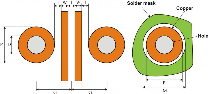
First of all you need to know where the board is manufactured. Basic information, we should know are:- The minimum track width - W,
- The minimum isolation gap - I,
- Minimum diameter of a Via (metal through-plated opening) - D.
Videos
What needs to be taken into account when designing the PCB to avoid interference? More about it in next article. Coming soon...
Always have the latest articles among the first. Subscribe to the newsletter.
Always have the latest articles among the first. Subscribe to the newsletter.
Useful links:
Do not miss these articles
Do you like our articles? Do not miss any of them! You do not have to worry about anything, we will arrange delivery to you.


